
Filtering plays an essential part in nearly all communication systems, since removing noise and distortion increases channel capacity. Designing a filter to pass only the desired frequencies is fairly easy. However, in real physical filter implementations there is a loss of desired signal power through the filter. This signal loss contributes decibel for decibel to the analog-to-digital converter (ADC) noise figure.
What may be even worse is that the amplifier driving the ADC will generate distortion at multiples of the filter loss. For example, if a filter has 7dB of loss, the amplifier needs to drive the signal 7dB stronger. This will result in second-order products with 7dB higher levels; third-order products will be 14dB worse. Some of these distortion products (intermodulation in particular) cannot be filtered out, so keeping filter loss to a minimum can be critical to system performance.
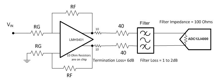
Figure 1: Typical signal chain
Selecting system components is also a key part of system design. Table 1 shows some ADCs, as well as their input specifications and an estimate for the amount of acceptable loss between the ADC and a typical 2Vpp amplifier output signal. The “Allowable filter loss” shown in the table is an arbitrary specification, but it will help select an ideal filter topology.
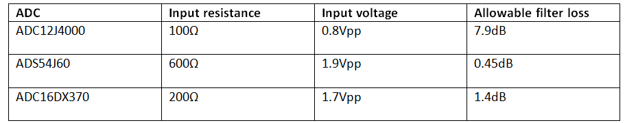
Table 1: ADC input parameters
Sources of filter loss
There are two types of filter losses: losses directly related to the filter components and losses associated with integrating the filter into the system. Filter component losses are nearly all due to parasitic resistance. In order to reduce component losses, minimize the equivalent series resistance (ESR) of the filter components.
While filter components ideally have no loss, the losses associated with integrating the filter into the system are more complex. Filters are designed to have an input and output impedance, which often requires resistors to provide a broadband impedance match, as shown in Figure 1. These matching resistors contribute a 6dB loss to the system voltage gain.
Reference measurements are another key consideration. While RF systems are usually designed around power levels, nearly 100% of available ADCs sample voltage and not power. For this reason, losses between the ADC driver amplifier and the ADC are usually specified in decibel volts instead of decibel power. This can be confusing, but it is important – because it is the loss in voltage that shows up in ADC measurements. Note that a 3dB loss in power equates to a 6dB loss in voltage.
Impedance transformation
Because the ADC samples voltage and not power, there is an opportunity to use the filter as a voltage gain circuit. This is possible because voltage and impedance are proportional for a given power level. The schematics shown in Figure 2 give one example of using a low-impedance input with a higher-impedance output to reduce overall loss by using the filter to step up the voltage. Figure 3 shows the results. The voltage loss drops 2.5dB. This approach works best when the ADC input impedance is 200Ω or higher. Looking at Table 1, this method would work with our 16-bit, 1-GSPS, dual-channel ADS54J60 and 16-bit, 370-MSPS, dual-channel ADC16DX370.
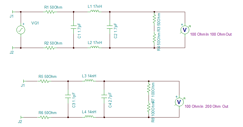
Figure 2: Filters with different impedance ratios
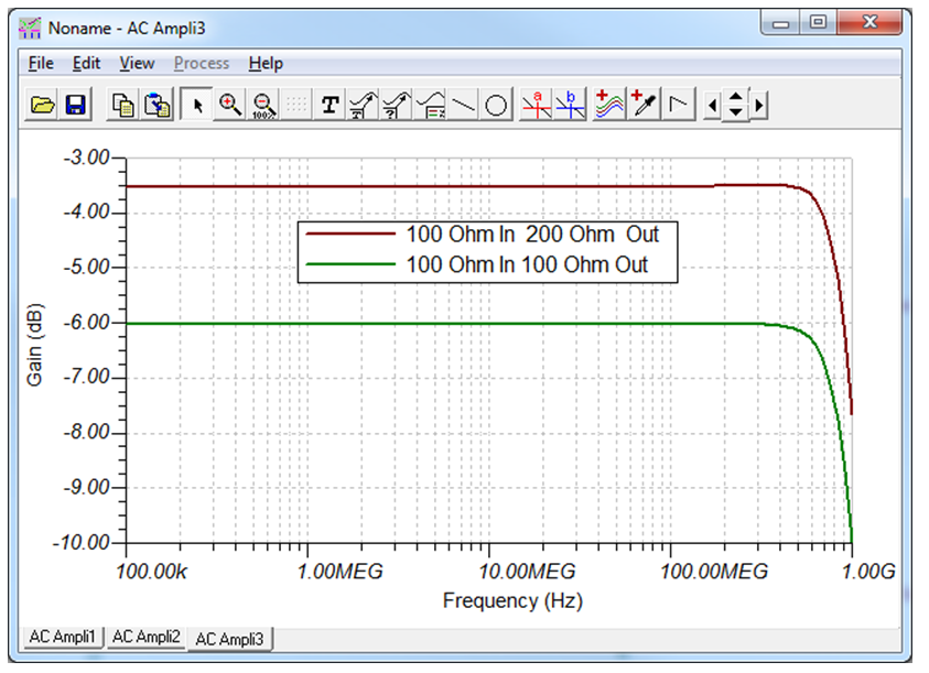
Figure 3: Filter responses for different impedance ratios
Decreasing the filter’s driving impedance
If the ADC’s differential input impedance is below 200Ω, increasing the filter’s termination resistance will not work well. Instead, try reducing the driving impedance into the filter as shown in Figure 4. Looking again at Table 1, this method would be suitable for the ADC16DX370 or ADC12J4000.
In the second circuit shown in Figure 4, removing the 40Ω resistors from Figure 1 reduces the driving impedance, which leaves the 10Ω internal resistors of the amplifier as the driving impedance. This reduces the filter loss but compromises the filter frequency response. Figure 5 has frequency response plots of properly terminated and mismatched filter responses.
With low-pass filters, you can adjust the filter corner frequency to recover the lost bandwidth, but with band-pass filters this is more difficult. Both pass-band flatness and adjacent-channel rejection will suffer with improper driving impedance.
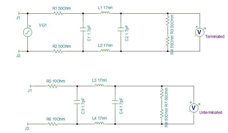
Figure 4: Filters with different driving impedances

Figure 5: Results with different driving impedances
Conclusion
Reducing the ESR losses of your filter’s reactive components and adjusting its driving and termination impedances helps manage signal loss when driving an ADC. The input impedance of the ADC limits the termination impedance of the filter, so careful ADC selection is critical. If you’d like some guidance with this, post your needs in the High-Speed Data Converter Forum or the High Speed Amplifiers Forum. Our experts can recommend an ADC that’ll be well suited for your system design and answer questions once you get started.
Additional resources
联系客服

