
In my first post, I introduced RS-485 and how it has become the preferred interface standard for many industrial fieldbus applications. In this and upcoming posts, I’ll cover fundamentals of RS-485 and addressing common application questions that arise when designing RS-485 networks. Many common RS-485 questions can be resolved with a basic understanding of the structure and operation of the driver and receiver. In this post, I’ll discuss the RS-485 driver and the relevant specifications in the RS-485 standard.

Figure 1: Differential output driver structure
Figure 1 shows the equivalent output schematic for the driver of TI’s SN65HVD72 half-duplex transceiver. The output structure consists of an H-bridge driver with high- and low-side transistors on each of the A and B outputs, which are in parallel with electrostatic discharge (ESD) cells on each terminal. The diodes in series with each transistor prevent reverse current flow from the bus terminals to the power supply if the voltage on A or B is greater than VCC, or from ground to the bus terminals if the voltage on A or B is below the ground potential.
The basic operation of the driver simplifies to the high and low output logic states, as shown in Figure 2 below.
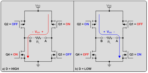
Figure 2: RS-485 output driver operation
The resulting waveform can be modeled as a positive and negative differential voltage superimposed onto a common-mode offset voltage, which is typically close to VCC/2, as shown in Figure 3.
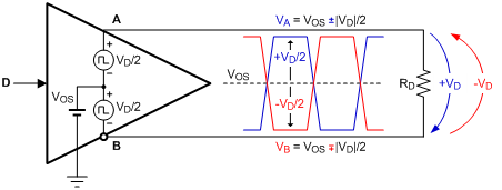
Figure 3: RS-485 driver output waveform
The RS-485 standard specifies that a compliant driver must produce a differential output voltage greater than 1.5V with a 54Ω load. The relevant RS-485 test circuit is shown in Figure 4 below.

Figure 4: RS-485 output driver test circuit
Therefore, the on-resistance of the high- and low-side transistors must be low enough to source sufficient current to produce 1.5V across 54Ω. A common rule of thumb is to assume a typical on-resistance of between 20Ω and 30Ω for each transistor.
Additionally, the RS-485 standard also requires that a compliant driver produce a differential output voltage greater than 1.5V with a 60Ω differential load and common-mode load of 375Ω from each of the A and B outputs to -7V to +12V.See an example of this below.
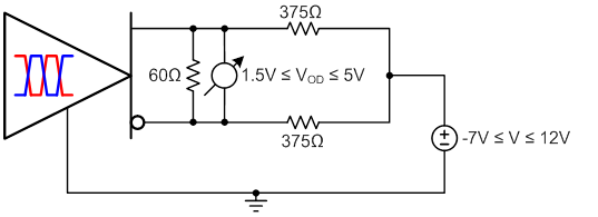
Figure 5: RS-485 output driver test circuit over common-mode
Further, the on-resistance of each leg of the H-bridge output must be well-matched (that is, Q1 ≈ Q2, and Q3 ≈ Q4). The RS-485 standard specifies that the difference in magnitude of VOD when the output is positive and VOD when the output is negative must be less than 200mV. When each leg of the H-bridge output is perfectly matched, this value, denoted as ∆|VOD| in the datasheet, is zero. For the SN65HVD72, ∆|VOD| has a maximum value of 50mV. Large imbalances in VOD for different logic states result in increased common-mode noise and higher levels of radiated electromagnetic interference (EMI).
A final important characteristic of any RS-485 driver is its output rise and fall time, which is determined by a separate circuit that controls the switching of transistors Q1, Q2, Q3, and Q4 (see Figure 2). The output rise and fall time limits the maximum data rate at which the transceiver can operate. Typically, the rise and fall time of the driver should be no more than one-third the total bit time at a given data rate. Further, for a given data rate, a transceiver with slower rise and fall times is preferable to a transceiver with faster rise and fall times, as it will radiate less electromagnetic interference (EMI) into adjacent circuitry.
Large differential output voltage and wide common-mode range differentiate RS-485 from other signaling standards and make it suitable for use in noisy electrical environments and applications, such as industrial automation, e-metering and motor control.
In the next installment of this series, I will discuss the design and basic operation of a typical RS-485 receiver.
Additional resources:
联系客服

