This application note describes how General Purpose Input/Output (GPIO) pins may be manipulated, from Linux, on various Simtec products and introduces the general concepts involved. This means this application note, with suitable allowances for specific hardware, applies to almost any ARM hardware. Although this note refers to Linux and MMU enabled processors the concepts and indeed implementation still apply to μCLinux.
The following sections will introduce the basic concepts of accessing peripherals on the ARM CPU and then move on to a practical realisation of these concepts under Linux. It should be noted that there already exist a good number of tools for accessing and manipulating GPIO, such tools should be used in preference to new code as they have been tested and proven.
Unlike other areas of software it is very possible to destroy hardware by misusing GPIO pins on a system and suitable care must be taken. Simtec cannot accept any liability for how this information is used.
All ARM processors access peripherals with memory mapped I/O. There are no specific instructions for manipulating I/O unlike some other processors like the Intel X86, instead all registers used to control a peripheral appear at some location in memory.
This introduces the first important issue to consider, that of alignment. The ARM CPU can only manipulate data on "naturally" aligned boundaries that is boundaries rounded to the same size as the datatype. For example a byte may be accessed on any byte alignment (with the LDRB instruction) a sixteen bit value may be accessed from any sixteen bit alignment (at address 0,2,4 but not 1,3,5) and a thirty two bit value (a word) may only be accessed on 32bit alignments (at address 0,4,8 but not 1,2,3)
The second issue to consider is access length, the access to the data must be exactly the correct length, this implies the data type of accesses from a typed language (such as C) must be correct. For example, to access a sixteen bit register a single access must be performed by the CPU, a pair of byte reads would cause two reads from the hardware and would probably cause completely incorrect results. The datasheet for the device being accessed should provide guidance on the width of the data being accessed.
The third major issue to consider is the locations of the registers within the CPU address space. Typically the registers will be specified in the devices datasheet in physical memory locations, that is addresses the CPU must physically present on its address bus to obtain access to the device. The Memory Management Unit (MMU) will almost always be active while an operating system is running and the logical addresses used by applications will have no relation whatsoever to the physical addressing scheme. Because of the MMU almost all OS provide a method of obtaining access to physical address space, these two forms of addressing should not be confused. Although not usually relevant for GPIO access sometimes designers will attach peripheral chips to address lines starting from the second or third address line, thus multiplying all accesses by two or four (indeed sometimes addresses of registers may be many megabytes apart) this is implementation specific but is common enough to mention as it is a source of confusion.
The final issue to consider is that of multiplexed or multifunction pins. There are a finite number of pins that can be attached to a physical processor package, most modern Processors are System on chip(SOC) type devices where there are a huge number of functions, often this means that there are many more possible signals than physical external pins. In order to deal with this GPIO pins are often multiplexed with other signals. A choice often has to be made between a special function signal or a GPIO, some devices may have more than one alternate function for a pin. The multiplexing on a pin is controlled by an additional register within the memory map.
There exist several ways of arranging GPIO signals in memory, by far the most common involves using a data register to hold a physical representation of the levels on the relevant GPIO pins and a data direction register which determines whether a given GPIO pin drives its output or reads a pin as input. This method provides for simple reading of the state of a pin but poses an issue when outputting values. Writing is performed using the Read Modify Write (RMW) scheme, this involves reading the current value of the data register, modifying the output bit (representing the external level) and writing the result back to the data register. If however this is not performed as an atomic operation and some other process performs its read during the modify time of the first when the values are written back the value of one of the processes will be lost, giving incorrect results.
ARM Linux provides a very simple way for user space applications to acquire access to Physical address space, while this is powerful, it may be dangerous as incorrect programming of hardware registers without the OS involvement will at best result in a crash and at worst damage to hardware. Care must be taken when manipulating hardware in this way and Simtec cannot accept responsibility for any errors made whilst using this information.
To access arbitrary addresses from userspace the /dev/mem file is used, this file allows a process to use the mmap call to obtain a user space pointer to a physical address. In this context mmap can only map complete pages. A general mapping of an arbitrary address is achieved using code such as this
#define MAP_SIZE 4096UL#define MAP_MASK (MAP_SIZE - 1)int main(int argc, char **argv) { int fd; void *map_base, *virt_addr; off_t target = 0xB7A01084; if((fd = open("/dev/mem", O_RDWR | O_SYNC)) == -1) { printf("/dev/mem could not be opened.\n"); exit(1); } else { printf("/dev/mem opened.\n"); } fflush(stdout); /* Map one page */ map_base = mmap(0, MAP_SIZE, PROT_READ | PROT_WRITE, MAP_SHARED, fd, target + & ~MAP_MASK); if(map_base == (void *) -1) { printf("Memory map failed.\n"); } else { printf("Memory mapped at address %p.\n", map_base); } fflush(stdout); virt_addr = map_base + (target & MAP_MASK); /* acess remapped region here */ if(munmap(map_base, MAP_SIZE) == -1) { printf("Memory unmap failed.\n"); } close(fd);} Once a mapping has been achieved the registers may be accessed as required, to ensure the correct type of access is performed by the CPU the void * pointer must be cast to the correct type, for instance in the above the following could be used
/* for a byte wide access */ read_result = *((volatile unsigned char *) virt_addr); /* for a sixteen bit access */ read_result = *((volatile unsigned short *) virt_addr); /* for a thirty two bit access */ read_result = *((volatile unsigned long *) virt_addr);
This code has been needed so often that the "devmem2" program gets referred to almost every time this subject occurs. The devmem2.c source code is a GPL program that allows memory to be manipulated from the command line. Whilst it cannot be directly copied into a non GPL program it should serve as an example of how this problem is solved correctly. As there is only one way to solve this problem correctly any resultant code will look very similar.
The major important areas here are
The first requirement is to be sure of the correct I/O pin used, as an example we shall use a simple switch circuit attached to an exposed GPIO line on our EB675001DIP module. We have chosen this as an example for the sake of clarity, but this explanation applies to any GPIO pin exposed on any of our boards.
The schematic fragment shown here has a simple switch circuit attached to IRQ1 and a simple LED circuit attached to the PWM0 output. These lines are labelled for their special functions, but as discussed earlier such lines are often multiplexed and referring to the EB675001DIP pinlist it can be seen IRQ1 is also the CPU PIOE[6] (This information could just as easily be taken from the OKI ML675001 manual). From the OKI ML675001 datasheet it can be seen that GPIO port E (PIOE) is controlled by six registers appearing at physical address 0xB7A01080 to 0xB7A01094 and in addition the GPCTL (0xB7000000) register.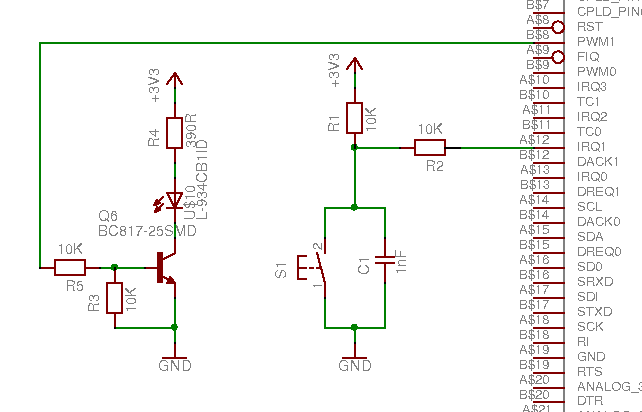
To cover all these registers a pair of single page mappings will suffice one at 0xB7000000 to cover the GPCTL register and one at 0xB7A01000 which will cover all the GPIO control registers.
Once the mappings have been performed the GPIO pin must be configured by setting or clearing the appropriate bits in the control registers. In our example this involves the following steps
After configuring the Pin its current status may simply be read from the port input register (GPPIE) at address 0xB7A01084 as the switch circuit is normally high the switch in its open state means bit 6 of the GPPIE register will be set, and when the button is pressed the bit will become cleared.
联系客服